What Is OSAT? How Chip Assembly and Testing Works in India
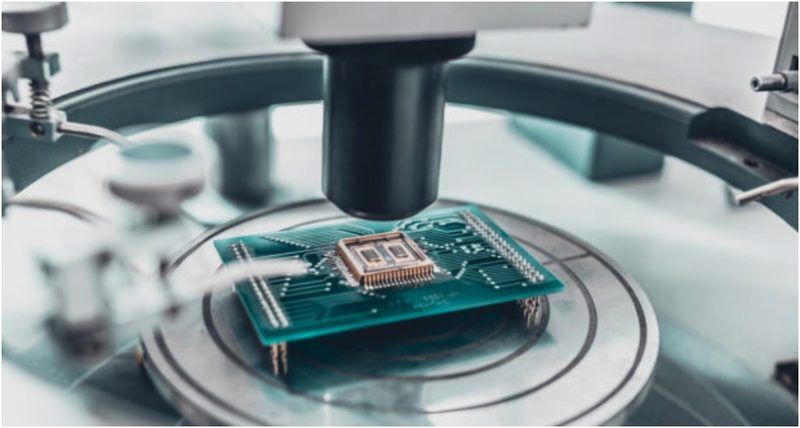
When people picture the semiconductor industry, they imagine the fab: billion-dollar cleanrooms printing transistors with ultraviolet light. But a silicon wafer full of chips is not yet a usable product. Each tiny die must be cut out, wired up, sealed into a protective package and rigorously tested before it can go into a phone or a car. That unglamorous final stage is called OSAT, Outsourced Semiconductor Assembly and Test, and it is where India is placing its biggest near-term bet in the chip race. Understanding OSAT explains how chips actually reach your devices, and why packaging has quietly become one of the industry’s hottest frontiers.
What does OSAT mean?
OSAT stands for Outsourced Semiconductor Assembly and Test: companies that specialise in the back-end steps of chip manufacturing for clients who designed the chips or fabricated the wafers elsewhere. The model mirrors the foundry idea: just as TSMC manufactures chips designed by Apple and Nvidia, OSAT firms like ASE, Amkor and JCET take finished wafers and turn them into packaged, tested chips. It is a huge industry in its own right, worth tens of billions of dollars, concentrated historically in Taiwan, Malaysia, the Philippines, Vietnam and China. The work is less famous than fabrication but absolutely critical: a brilliantly designed chip is worthless until it is packaged and proven to work.
How does chip assembly work?
The process starts where the fab ends. The finished wafer is thinned, because a thinner die means a thinner phone, then diced into individual chips with diamond saws or lasers. Each die, often just millimetres across, is picked up by precision robots and attached to a substrate or lead frame, the base that will carry its external connections. Then comes wire bonding or flip-chip attachment: microscopic gold or copper wires, finer than a human hair, connect the chip’s contact pads to the package leads, or the chip is flipped face-down onto solder bumps for denser connections. The assembly is then encapsulated in protective epoxy moulding, marked with laser engraving, and fitted with solder balls or pins. Modern advanced packaging goes further, stacking memory directly on processors or joining multiple chiplets side by side, techniques now so important that packaging innovation rivals transistor shrinking as a source of progress.
How are chips tested?
Testing happens at multiple stages because catching a bad chip early saves money. Wafers are probed electrically before dicing, and known-bad dies are mapped and discarded. After packaging, automated test equipment runs each chip through functional tests at various temperatures and voltages, checking that it performs to specification. Chips are “binned”: the best become premium processors, slightly weaker ones are sold as lower-tier parts, and failures are scrapped. For automotive and industrial chips, testing includes burn-in, running chips hot for hours to weed out early failures, because a chip in a car’s braking system cannot be allowed to fail. Test engineering is a discipline of its own, and test capacity is a genuine bottleneck: during shortages, finished wafers have waited months for test slots.
Why is India betting on OSAT?
India’s semiconductor strategy leads with OSAT for pragmatic reasons.
- Cost and speed: an OSAT facility costs hundreds of millions, not the tens of billions a leading-edge fab demands, and can be built in a couple of years.
- Talent pipeline: assembly and test builds the skilled workforce, engineers and technicians, that a future fab will need.
- Supply chain logic: packaging chips in India serves the country’s booming electronics manufacturing, from phones to automobiles.
- Global diversification: chipmakers want packaging outside the traditional hubs, and India offers scale, stability and incentives.
- Technology trend: advanced packaging is where much of the industry’s innovation now happens, so OSAT is not the low-tech consolation prize it is sometimes portrayed as.
Projects announced under the semiconductor mission, including a major Tata facility in Assam, aim to put India on the OSAT map within the next few years.
What are the challenges?
OSAT is more accessible than fabrication, but it is not easy. The business runs on thin margins and enormous volumes, so operational excellence matters more than anywhere. Customers demand certifications and proven yields before trusting a new facility with their wafers. The supply chain for substrates, lead frames, moulding compounds and test equipment must be built alongside the plants. And while OSAT is the right first step, India will eventually need the full stack, design, fabrication, packaging, to capture the industry’s real value. The honest assessment: OSAT is the foundation course, necessary and valuable, but not the degree.
FAQs
Is OSAT “real” chip manufacturing? Yes. It is an essential, technically demanding stage without which no chip reaches a product. The industry’s growing focus on advanced packaging has only raised its importance.
How long before India’s OSAT plants produce chips? Typical timelines run two to three years from groundbreaking to volume production, with customer qualification adding months more.
What jobs does OSAT create? Thousands per facility: process engineers, test engineers, technicians, quality specialists and supply chain roles, plus construction and indirect employment.
The next time you hold a phone, remember the chip inside survived a journey most people never see: grown as a crystal, printed with light, then cut, wired, sealed and tested before it ever met a circuit board. OSAT is where silicon becomes product, and India’s bet is that this is exactly where its semiconductor story should begin.
Compiled by the Khabar 24h Editorial Desk from publicly available sources.

Khabar 24h Editorial Desk — our explainers are prepared by the Khabar 24h editorial team using AI-assisted research tools, and every piece is reviewed by a human editor before publishing. We do not claim original reporting: our work is turning complex topics into simple, accurate summaries. Spotted an error? Write to contact@khabar24h.com — our corrections policy aims for same-day review.
More from this author →