What Does 3nm Mean? How Chip Manufacturing Nodes Work
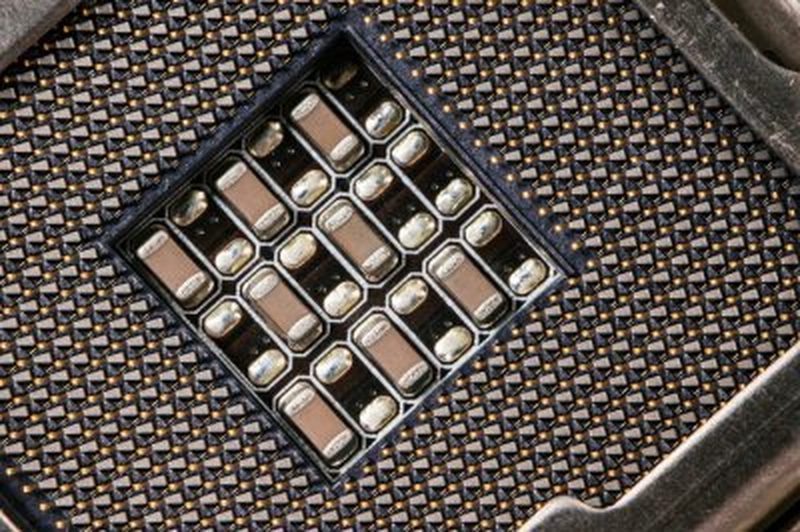
Every new phone launch brings the same boast: a chip built on a “3nm process”, faster and more efficient than last year’s 5nm. The numbers sound precise, like measuring a transistor with a ruler, and they drive billions of dollars in investment and national pride. But here’s the industry’s open secret: 3nm does not mean transistors 3 nanometres wide. The naming of chip manufacturing nodes has become marketing as much as measurement. Understanding what process nodes really are, how they evolved, and what the numbers actually tell you, cuts through the hype to what matters for your devices.
What is a process node?
A process node is a generation of chip manufacturing technology. Each new node historically shrank transistors, letting chipmakers pack more of them onto the same silicon, which made chips faster, cheaper per transistor and more power-efficient all at once. This was the engine of Moore’s Law, the observation that transistor counts doubled roughly every two years. For decades the node name matched a real physical dimension: the “90nm” node of the early 2000s really did have key features about 90 nanometres wide. Nodes marched downward, 65nm, 45nm, 32nm, 22nm, 14nm, each a genuine shrink. Then, around the 10nm mark, the naming broke from physical reality, and the numbers became what engineers privately call “marketing nodes”.
Why doesn’t 3nm mean 3 nanometres?
Modern transistors are three-dimensional structures, FinFETs and now gate-all-around designs, whose critical dimensions cannot be captured by a single number. When the industry reached the limits of simple shrinking, foundries kept the familiar countdown going for commercial reasons: “3nm” signals a new generation denser and more efficient than “5nm”, even though no mainstream feature on the chip measures 3 nanometres. Actual transistor features on a “3nm” chip are typically in the teens of nanometres. Worse, different foundries’ nodes are not comparable: one company’s “3nm” may be denser than another’s, and Intel renamed its own nodes to match the industry’s numbering. The honest way to compare nodes is transistor density, how many transistors fit per square millimetre, and power efficiency, not the headline number.
How are smaller nodes actually made?
Each node generation demands new manufacturing tricks. Extreme ultraviolet lithography, pioneered for the 7nm generation and essential at 5nm and 3nm, uses 13.5-nanometre light to print features that older techniques cannot resolve. Transistor architecture changed too: FinFETs raised the transistor channel into a 3D fin for better control, and the newest gate-all-around transistors wrap the gate completely around stacked silicon sheets, cutting leakage current. New materials appear at every step, cobalt and ruthenium interconnects, novel insulating films. Each advance requires re-engineering hundreds of process steps and billions in R&D, which is why only three companies, TSMC, Samsung and Intel, still compete at the leading edge. Everyone else buys from them.
What do smaller nodes mean for your phone?
For users, node advances translate into three tangible benefits.
- Battery life: smaller, more efficient transistors do the same work with less power, which is why phones keep gaining performance without gaining bulk.
- Performance: higher density lets designers add more CPU and GPU cores and larger AI accelerators, powering on-device AI features.
- Heat: efficient chips run cooler, sustaining peak performance longer during gaming or video recording instead of throttling.
- Cost, eventually: more chips per wafer means lower cost per chip, though leading-edge wafers are so expensive that savings take years to reach consumers.
The gains are real but diminishing: the jump from 5nm to 3nm brings roughly 15 to 30 per cent better efficiency, meaningful, but not the doubling leaps of the old days.
What comes after 3nm?
The roadmap continues: 2nm-class nodes are entering production with gate-all-around transistors and a new technique called backside power delivery, which routes power from beneath the chip to reduce congestion. Beyond that, the industry talks about “angstrom-class” nodes, 18A, 14A, abandoning nanometres for angstroms, a tenth of a nanometre, purely as labels. Longer term, engineers are stacking transistors vertically, exploring new channel materials, and pursuing chiplet designs that combine multiple specialised dies instead of one giant shrinking monolith. The node number will keep shrinking on marketing slides; the real progress will be measured in watts, transistors per square millimetre, and what your devices can actually do.
FAQs
Is a 3nm chip always better than a 5nm chip? Not necessarily. Architecture, design quality and software matter enormously; a well-designed 5nm chip can beat a mediocre 3nm one. The node is one ingredient, not the whole recipe.
Why do only three companies make leading-edge chips? Each node generation costs tens of billions in R&D and fab construction. The economics only work at enormous scale, which has concentrated the industry into TSMC, Samsung and Intel.
Will Moore’s Law continue? Transistor counts keep rising through new architectures and 3D stacking, but the era of cheap, easy shrinks is over. Progress continues; it just costs more.
So the next time a launch event trumpets “3nm”, you will know the truth: the number is a generation label, not a measurement. What matters is what the generation delivers, more efficient transistors enabling faster phones, longer battery life and smarter on-device AI. The nanometres are marketing; the progress is real.
Compiled by the Khabar 24h Editorial Desk from publicly available sources.

Khabar 24h Editorial Desk — our explainers are prepared by the Khabar 24h editorial team using AI-assisted research tools, and every piece is reviewed by a human editor before publishing. We do not claim original reporting: our work is turning complex topics into simple, accurate summaries. Spotted an error? Write to contact@khabar24h.com — our corrections policy aims for same-day review.
More from this author →